
Figure 1

|
Figure 1 |
PSPICE is a widely used circuit simulation program. It allows circuits too be tested and debugged before they are built. Sometimes the cost of fabricating a circuit can be quite large, especially if it is being fabricated on an integrated circuit chip. Simulations improve the probability of success on the first try.
PSPICE. is FREE and available on-line. It runs on your PC.
PSPICE Users Guide and the Capture Users Guide are valuable references.
We will simulate the circuit shown in Figure 1.
Open Schematic Capture.
Computers differ, but on my computer I used,
Start > All Programs > PSpice Student > SchematicsAs shown in Figure 2.
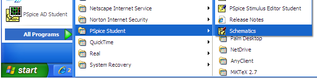

Figure 3 Draw window
|
Place a resistor. Use,
Draw > Get New PartRotate a selected resistor 90 degrees by pressing control-r. A selected component is highlighted in red.
Type R in the Part Name box. Then select Place.
Move the cursor to the place you want to place the resistor.
Click to place the resistor.
Move the cursor to the place you want to place a second resistor and click.
Double click to place the last resistor and exit from resistors.
Place a DC power source. Use Draw> Get New Part and type V in the Part Name box.
Select and place circuit elements VDC and AGND.
AGND identifies the reference (ground) node in the circuit. Every SPICE circuit must have a reference node.
Position the parts and connect them with wires. Type control-w to get the wire tool. Click to start and end a wire. Double click to exit the wire tool.
Notice the resistor values are 1K. Double click on the 1K label to get the Set Attribute box. Enter the correct the new resistance value. Do this for all resistors.
Also, place the component IPROBE in wires to measure current and the component VIEWPOINT at nodes to measure voltages.
IPROBEs appear as meters in the schematic (Figure 6).
The meters will register negative currents if they are in backwards.
To rotate, select and type control_r.
VIEWPOINTS appear as triangles pointing to nodes in the schematic.
We have also labeled nodes by double clicking on wires. A window comes up where we can enter the node label. Double click on a wire to label it.. In the Set Attribute box, enter the desired label,
Save the design.
Now create a netlist (PSPICE input file) using the Analysis pulldown menu and selecting Create Net List.
Look at the netlist using the Examine Netlist in the Analysis pulldown menu.
 | Figure 5 The PSpice netlist is shown. A line beginning with 'V' represents a voltage source. The syntax is "Name, node 1, node 2, value". V_V1 in 0 10 represents the 10 Volt source connected between ground (0) and node 'in'. A line beginning with R represents a resistor. Notice $N_0001 is a node label created by PSpice for a node we did not label. The ammeters are zero valued voltage sources. |

